A major milestone in propelling industry into the Ångstrom era
, /PRNewswire/ — Today, imec, a world-leading research and innovation hub in advanced semiconductor technologies, announces the arrival of the ASML EXE:5200 High NA EUV lithography system, the most advanced lithography tool available today. With this strategic milestone, imec reinforces its position as the industry’s launchpad into the angstrom era, giving its global partners ecosystem unparalleled early access to the next generation of chip-scaling technologies. Integrated directly with a comprehensive suite of patterning and metrology tools and materials, the High NA EUV system will empower imec and its ecosystem partners to unlock the performance needed to pioneer sub-2nm logic and high-density memory technologies that will fuel the rapid growth of advanced AI and high-performance computing.
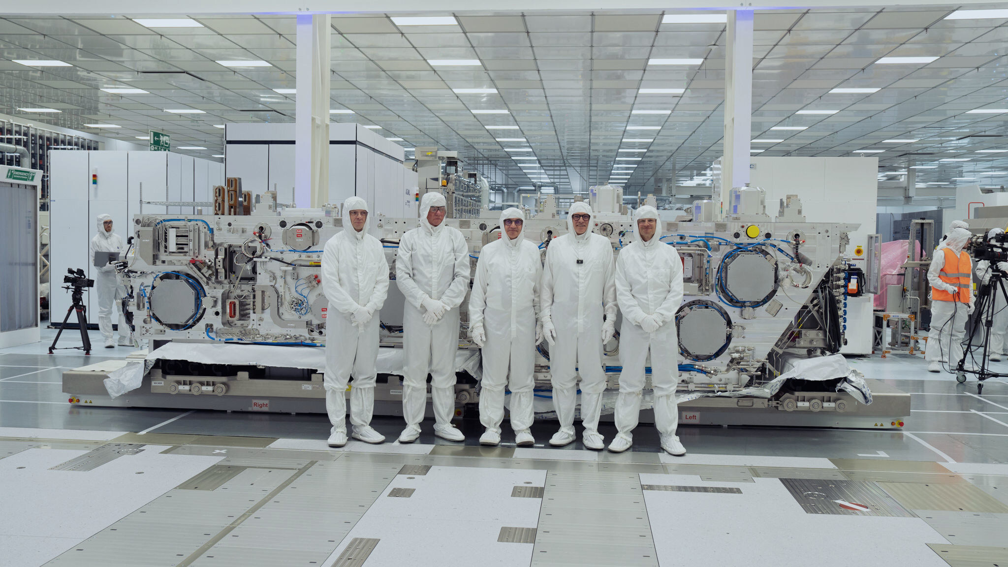
, Martin van den Brink (ASML), Luc Van den hove (imec), Matthias Diependaele (Flemish government), Patrick Vandenameele (imec)")
Luc Van den hove, CEO of imec: “The past two years have marked an important chapter for High NA (0.55NA) EUV lithography, with imec and ASML joining forces with the ecosystem in its joint High NA EUV Lithography Lab in Veldhoven (The Netherlands) to pioneer High NA EUV technology. With the installation of the EXE:5200 High NA EUV lithography system into our 300mm cleanroom in Leuven (Belgium), we aim to bring these High NA EUV patterning technologies to an industry-relevant scale and to develop the next-generation High NA EUV patterning use cases. Its unmatched resolution, improved overlay performance, high throughput, and a new wafer stocker that improves process stability and throughput, will give our partners a decisive advantage in accelerating the development of sub-2nm chip technologies. As the industry moves into the Ångstrom era, High NA EUV will be a cornerstone capability, and imec is proud to lead the way by offering its partners the earliest and most comprehensive access to this technology.”
This milestone is a key element of imec’s five-year strategic partnership with ASML supported by the EU (Chips Joint Undertaking and IPCEI), the Flemish government, and the Dutch government. Luc Van den hove: “As an integral part of the EU funded NanoIC pilot line, the tool is set to play a pivotal role in strengthening Europe’s position as a leader in advanced semiconductor R&D in the decades to come.”
Having the ASML EXE:5200 High NA EUV lithography system in imec’s cleanroom firmly positions imec as the most comprehensive development environment for advanced patterning. Imec’s deep ecosystem collaboration with leading chip manufacturers, equipment, material and resist suppliers, mask companies, and metrology experts will allow us to ramp up learning cycles and enhance process stability to develop and demonstrate cutting-edge patterning for next generation logic and memory device technology, driving breakthroughs that will shape the future of advanced computing and AI in the years to come.
Christophe Fouquet, CEO of ASML: “Imec’s installation of the EXE:5200 marks an important step into the Ångstrom era. Together, we’re accelerating High NA EUV extendibility for the next generations of advanced memory and compute.”
Imec anticipates the EXE:5200 High NA EUV lithography system to be fully qualified by Q4 2026. In the meantime, the joint ASML-imec High NA EUV lithography Lab in Veldhoven will remain operational, ensuring continuity in the High NA EUV R&D activities for imec and its ecosystem partners.
About imec
Imec is a world-leading research and innovation hub in advanced semiconductor technologies. Leveraging its state-of-the-art R&D infrastructure and the expertise of over 6,500 employees, imec drives innovation in semiconductor and system scaling, artificial intelligence, silicon photonics, connectivity, and sensing.
Imec’s advanced research powers breakthroughs across a wide range of industries, including computing, health, automotive, industry, consumer electronics, aerospace and security. Through IC-Link, imec guides companies through every step of the chip journey – from initial concept to full-scale manufacturing – delivering customized solutions tailored to meet the most advanced design and production needs.
Imec collaborates with global leaders across the semiconductor value chain, as well as with technology companies, start-ups, academia, and research institutions in Flanders and worldwide. Headquartered in Leuven, Belgium, imec has research facilities in Belgium, across Europe, the USA and the GCC region, and representation on three continents. In 2024, imec reported revenues of €1.034 billion.
For more information, visit www.imec-int.com
The imec group holds a global trademark portfolio, including word marks and combined figurative registered and unregistered trademarks, across national, regional, and international territories. Its lawful use requires prior written consent of IMEC in compliance with the IMEC branding guidelines, which may be updated periodically. The latest version is available upon written request.
SOURCE Imec